Improving the Design Process of a MEMS-IR-Emitter
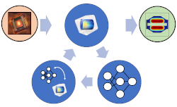
In the rapid development cycle of sensor systems, minimizing time-to-market is crucial. However, designing a new MEMS-chip (Micro-Electro-Mechanical Systems) presents significant challenges due to the extensive time required for manufacturing and characterization. This delay affects the development of dependent components, such as control electronics, which rely on understanding the operational conditions of the MEMS-chip. The development cycle for a MEMS chip involves significant time investments, with silicon chip manufacturing taking several weeks or months, followed by at least another six months dedicated to lifetime analysis and characterization. Establishing a reliable lifetime model for a chip expected to last over five years (exceeding 50,000 hours) necessitates accelerated aging tests spanning around 5,000 hours (roughly 6-7 months). This statistical analysis requires extensive data and numerous samples, often demanding additional data to account for environmental conditions, further prolonging the process. Consequently, there is typically a year-long gap between chip design and the determination of its optimal operational conditions, which are critical for the development of dependent components like control electronics. Two critical factors must be addressed to expedite this process to allow parallel development of dependent components: ensuring the design to be manufactured meets the functional expectations robustly and accurately, and estimating the operational parameters. Achieving narrower boundaries for these conditions enhances the efficiency of the overall development process. In our approach, we established a comprehensive model of a MEMS-IR-emitter chip. With an algorithm including the basic model and experimental data we were able to identify the necessary material parameters by solving this inverse problem using a neural network. This model was validated with further experimental data. Moreover, we were able to implement a metric to monitor the primary aging failure mechanism electromigration. With the experimentally validated model, which functions as a digital twin of our MEMS-IR-emitter technology, we can analyze how design parameter variations influence emitter functionality, specifically its radiosity, lifespan, and dynamic behavior (see fig. 1). This capability allows us to simulate modifications ranging from minor adjustments in existing chip designs to the development of new emitters tailored for specific requirements. Furthermore, by employing a surrogate model, we can accurately evaluate the ideal operational conditions for the designed chip (see fig. 2). This precise estimation enables the parallel development of other components, such as control electronics, alongside the chip manufacturing process. This integrated simulation and modeling approach significantly reduces the time required to develop a MEMS-chip and its dependent components, thereby accelerating the overall product development cycle. In conclusion, leveraging advanced simulation and modeling techniques, including neural networks and surrogate models, allows us to streamline the MEMS-chip development process. By accurately predicting operational conditions and enabling parallel development of dependent components, we can significantly shorten the time-to-market for new sensor systems.

Téléchargement
- schildhauer_9631_poster.pdf - 1.3MB
- 3_toni_schildhauer.pdf - 2.55MB
