Aperture Shape Optimization for Electroplating of a Printed Circuit Board
Application ID: 139551
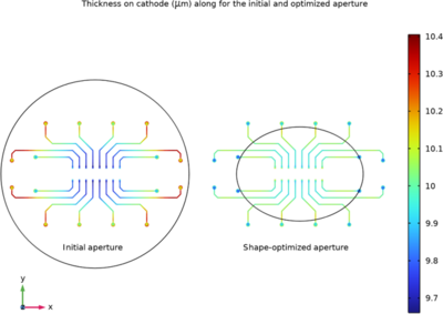
An aperture is often used in electroplating baths in order to improve the uniformity of the deposited metal layer.
This example simulates electroplating of a printed circuit board (PCB) in 3D using a secondary current distribution. The size and aspect ratio of the aperture is optimized using the Shape Optimization interface.
This model example illustrates applications of this type that would nominally be built using the following products:
however, additional products may be required to completely define and model it. Furthermore, this example may also be defined and modeled using components from the following product combinations:
- COMSOL Multiphysics® et
- Module ECAD Import et
- soit le Module Battery Design, Module Corrosion, Module Electrochemistry, Module Electrodeposition, ou Module Fuel Cell & Electrolyzer
The combination of COMSOL® products required to model your application depends on several factors and may include boundary conditions, material properties, physics interfaces, and part libraries. Particular functionality may be common to several products. To determine the right combination of products for your modeling needs, review the Grille des Spécifications and make use of a free evaluation license. The COMSOL Sales and Support teams are available for answering any questions you may have regarding this.