Advanced Semiconductor Modeling
Part 3 of this semiconductor modeling course focuses on more advanced semiconductor modeling concepts. First, we cover carrier mobility models that are used to simulate semiconductor devices with a drift-diffusion approach. In these cases, the mobility is limited by a scattering of carriers within the model. The predefined mobility models include options for photons, ionized impurities, carrier-carrier scattering, neutral impurity scattering, high field velocity saturation and surface scattering. Following this, we discuss how to use the density-gradient formulation for the effects of quantum confinement in the conventional drift-diffusion formulation without requiring excessive additional computational costs.
Demo: Mobility Models and Breakdown
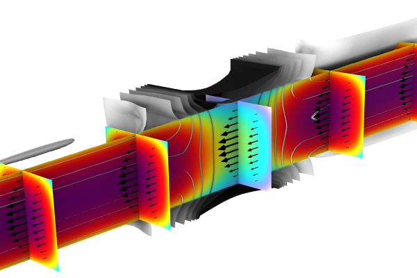
Here we will expand on the MOSFET tutorial model we introduced in the last section. First, we will walk you through the general features of the basic MOSFET model. You can add on electrical breakdown and more complex mobility models, as well as look at the small-signal AC response. We will look at each of these more advanced features separately.
- To demonstrate the electrical breakdown, we use a time-dependent study and add a time-dependent voltage ramp and an impact ionization generation.
- To demonstrate mobility models, we use a stationary study and add the Arora, Lombardi Surface Mobility and Caughey-Thomas Mobility Models
- To demonstrate small-signal AC response, we apply a DC voltage with a small AC perturbation by starting with a stationary study and adding a Frequency-Domain Perturbation study step, as well as a Harmonic Perturbation subfeature on one of the metal contacts
Demo: Quantum Confinement and Density Gradient Formulation
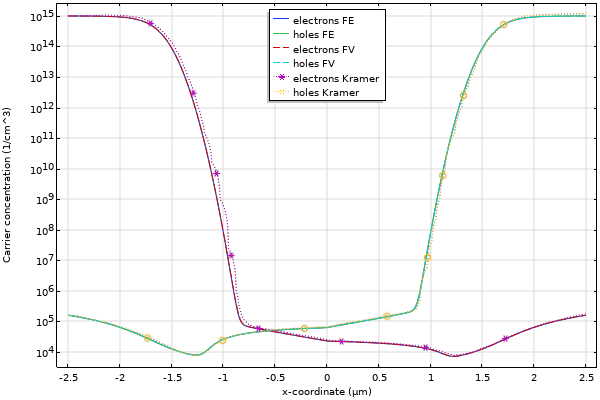
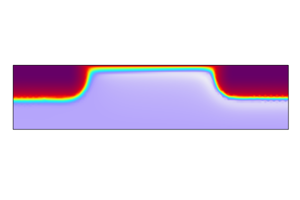
Below, we showcase how to use the density gradient formulation to add the effect of quantum confinement to the conventional drift-diffusion formulation. The density gradient formulation is an approximation used for quantum confinement models in nanometer scale semiconductor devices. The oxide layer is simulated explicitly with geometric domains and quantum confinement is at the silicon-oxide interface is accounted for by using a Potential Barrier option for the Insulator Interface boundary condition. For the full derivation of the density gradient formulation, see the documentation referenced in the Further Learning section.
Further Learning
- Documentation
- COMSOL Documentation – chapter on the Semiconductor Module > User's Guide > Semiconductor Branch Interface > Theory for the Semiconductor Interface > Boundary Conditions for the Density-Gradient Formulation
- Blog post
- Application Gallery
Envoyer des commentaires sur cette page ou contacter le support ici.

