Tunnel Diode
Application ID: 104361
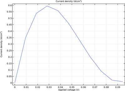
This tutorial demonstrates how to model the band-to-band tunneling across a p–n junction. The tunneling effect is imitated by defining the User-Defined Recombination domain feature which makes the electrons disappear from the conduction band on the n-side and holes disappear from the valence band on the p-side. The resulting J–V curve (current density vs. applied voltage) under forward bias is derived from the model.
This model example illustrates applications of this type that would nominally be built using the following products:
however, additional products may be required to completely define and model it. Furthermore, this example may also be defined and modeled using components from the following product combinations:
The combination of COMSOL® products required to model your application depends on several factors and may include boundary conditions, material properties, physics interfaces, and part libraries. Particular functionality may be common to several products. To determine the right combination of products for your modeling needs, review the Grille des Spécifications and make use of a free evaluation license. The COMSOL Sales and Support teams are available for answering any questions you may have regarding this.