
In 1980, Eli Yablonovitch from Bell Communication Research pondered how to reduce losses in semiconductor lasers in a specific frequency range. He sliced periodic circular holes in a transparent medium and observed that it didn’t allow the frequency range causing the losses to pass through. Yablonovitch found that these structures work similarly to semiconductors with conduction and valence bands and named them photonic crystals (with Sajeev John from Princeton University). Let’s discuss three examples in which photonic crystals control light.
Editor’s note: This blog post was updated on November 18, 2020, to reflect updated modeling functionality.
Introducing the Photonic Crystal
Photonic crystals are optical structures that periodically repeat to achieve different applications, such as bending light, filtering, and mirrors. One of the simplest configurations of a photonic crystal is to set up two different dielectric materials that are repeated periodically in a single direction (+/- Y direction in this model), also known as multilayer film. We perform three different analyses for a 1D photonic crystal based on the relative permittivity of the two layers (blue and green), as discussed in Chapter 4 of Ref. 1.
- Case 1:
= 13 and
= 13
- Case 2:
= 13 and
= 12
- Case 3:
= 13 and
= 1
For simplicity, instead of modeling the actual 3D geometry with multilayer film repeating in a single direction, a 2D cross section geometry is modeled. The Floquet periodic condition is applied in the +/- Y direction, while the Continuity periodic condition is applied in the +/- X direction of the photonic crystal. The Continuity periodic condition allows the unit cell to be extended to infinity in the +/- X direction by applying the same solution to the source and destination boundaries. While the Floquet periodic condition allows the infinite repetition of the unit cell in +/- Y direction by applying appropriate phase variation between the source and destination boundaries.
The eigenfrequency analysis is performed with the wave vector (ky) swept from to
, where a is the thickness of the layer (200 nm in this model). The eigenfrequency analysis is performed around 100 THz, and a higher number of eigenfrequencies are searched for (8 in this model). The dispersion relation can be plotted for each of the cases using a “freq” expression, which represents the eigenfrequency.
From the dispersion relation, it can be inferred for the first case, where the material properties are considered to be homogeneous, the modes lie along the light line . In the second case, the slight change in the relative permittivity results in the formation of the photonic bandgap between 105 THz and 107 THz. For the third case, due to the significant difference in the relative permittivity, the photonic bandgap spreads further, rejecting the frequencies between 114 THz and 192 THz, eventually working as a filter.
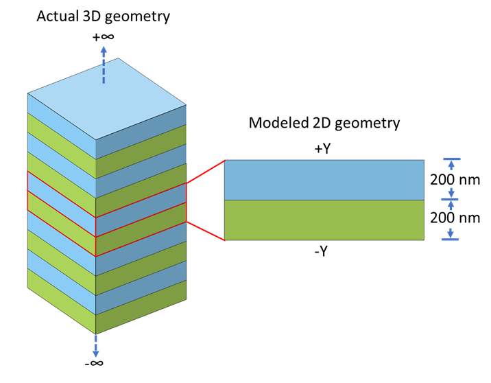
Schematic of actual 3D geometry of 1D photonic crystal and the modeled 2D geometry in COMSOL Multiphysics.

Dispersion analysis for the three cases of the 1D photonic crystal.
Bending Light with a Photonic Crystal
When GaAs pillars are arranged in a periodic manner, as shown in the figure below, the device has the ability to bend light with an angle (90° in this case) and also act as a filter for a band of frequencies (also called a photonic band gap).
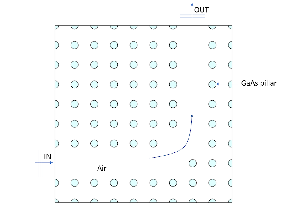
Schematic of a photonic crystal.
To model this photonic crystal in the COMSOL Multiphysics® software and add-on Wave Optics Module, the transverse electric (TE) wave (polarized in the z direction) is made to propagate through the left boundary using the Scattering boundary condition and an amplitude of 1 V/m. The rest of the boundaries are assigned Scattering boundary conditions with no incident fields. When we run the model with a sweep of different wavelengths for the incident light source, we get a graph of the transmittance and reflections, as shown below.
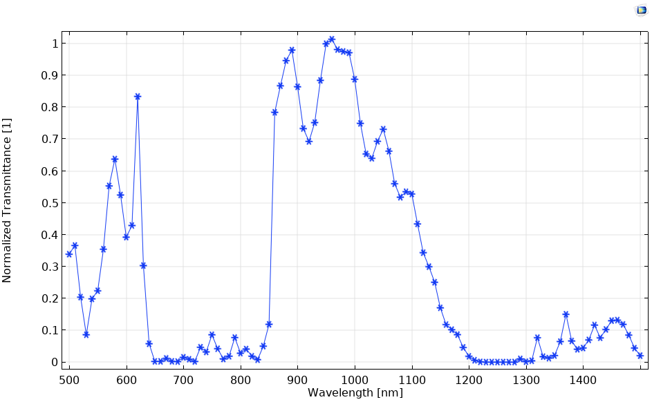
Normalized transmittance of the photonic crystal.
Left: Passband at a 1000-nm wavelength. Right: Stopband at a 700-nm wavelength.
Modeling a Photonic Crystal Fiber
A step-index fiber guides light through the high refractive index of the core, while a photonic crystal fiber (PCF) is made up of microstructured optical fibers that guide light either through index guiding or band gap confinement. In this blog post, we focus on index-guided PCF, where the core of the PCF is made of cladding material and is surrounded by air-filled holes. We assume the air hole’s radius as 0.3*pitch, where the pitch is the distance between adjacent holes. To quantify the dispersion relationship, the mode analysis is performed using the 2D cross section of this photonic crystal fiber, assuming the wave propagation to occur in out of plane direction.
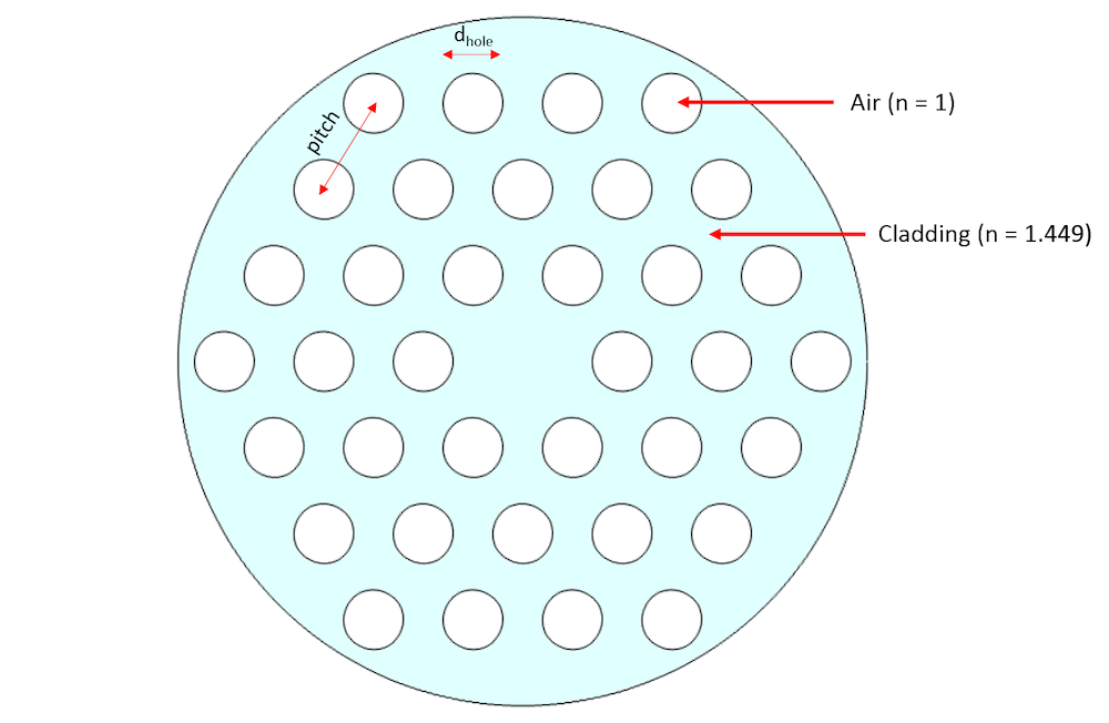
Schematic of index-guided photonic crystal.
To plot the dispersion diagram (the effective refractive index vs. the normalized wavelength), we perform a mode analysis along with a parametric sweep over the hole radius from 0.23 um to 4.69 um. To detect the fundamental and higher-order modes, the number of modes to search is increased to 50. The challenge then becomes correctly identifying the fundamental and higher-order modes from a total of 50 identified modes. One approach to identify these modes is to perform an integration in the core region for different effective mode indices (or effective refractive indices).
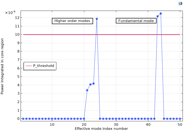
Power integrated in the core region vs. the effective mode index number for a 4.65-um hole radius and 15.5-um pitch.
There are two approaches to filter out unnecessary modes and capture only the meaningful fundamental and higher-order modes:
- Apply a filter to the power; for example, the required effective refractive index is then
ewfd.neff*(intop1(ewfd.Poavz)>P_threshold), whereP_thresholdis the power that will eliminate the unnecessary modes - Observe the effective mode index number for the fundamental and higher-order modes and if it is getting repeated
In this case, we observe that the fundamental mode is repeated between effective mode index numbers 40 and 45, and higher-order modes were repeated between effective mode index numbers 20 and 25. The dispersion diagram is plotted by included both of these filters to remove the unnecessary modes. The dispersion diagram matches well with Figure 4, Chapter 9 in Ref. 1.
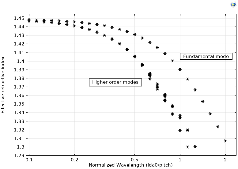
Dispersion diagram: effective refractive index vs. normalized wavelength (lda0/pitch).
In another example, the leaky modes of the microstructured optical fiber are analyzed. The mode analysis is performed to quantify the complex effective refractive index of different modes, such as HE, TE01, and TM01-like modes. The mode analysis uses Mode search method as Region and explicitly mentions the smallest and largest values of the real and imaginary parts of the refractive index. The perfectly matched layer (PML) along with the Scattering boundary condition (SBC) are used to truncate the simulation domain.
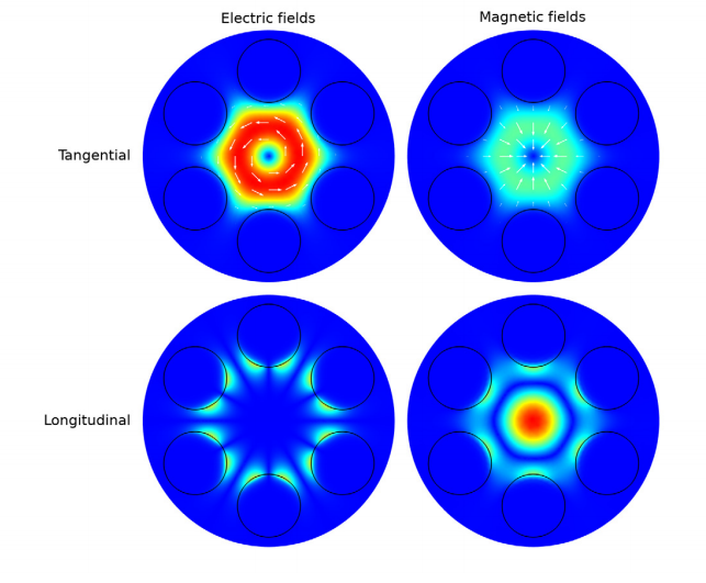
TE01-like mode of the microstructure optical fiber.
Analyzing a Photonic Band Gap
An alternate approach to modeling the band gap is to formulate an eigenvalue problem, as shown in the Band Gap Analysis of a Photonic Crystal model. In this case, a periodic arrangement of GaAs pillars is modeled in which the pillars are placed equidistant from each other. Instead of modeling an array of GaAs pillars, as we did in the first example, we model only a single unit cell and apply a Floquet periodic boundary condition, as shown below.
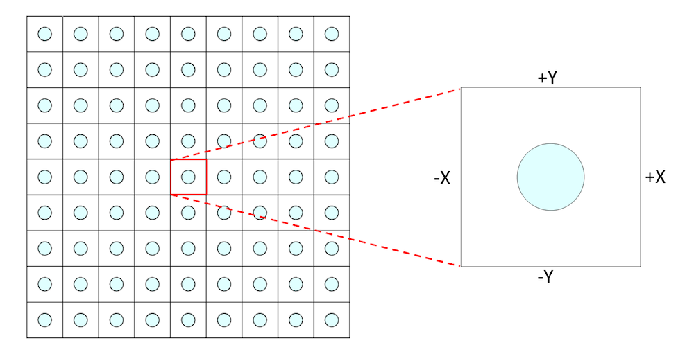
Array to unit approximation with the Periodic boundary condition applied at +/- X and +/-Y.
An auxiliary sweep is performed on the wave vector k from 0 to 0.5 to evaluate the dispersion relation in the (1,1) direction. Additionally, the refractive index of the GaAs material is considered frequency dependent. As can be seen below from the dispersion relationship, there is no EM wave propagation surviving in the (1,1) direction between bands 3 and 4, also known as the band gap of the photonic crystal.
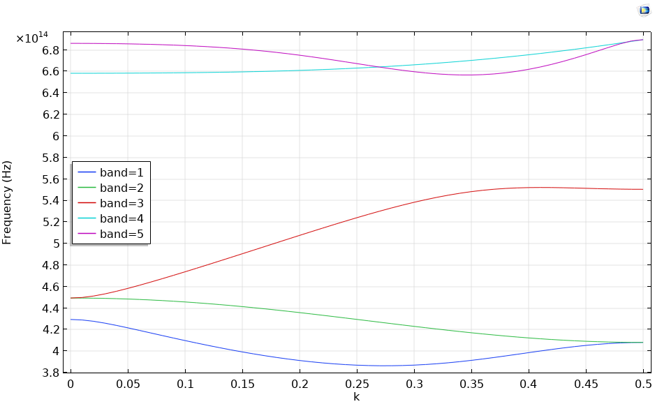
Dispersion relation when the wave vector is varied from 0 to 0.5 in the (1,1) direction.
Final Thoughts on Photonic Crystals
There are different approaches to modeling photonic crystal devices, whether you perform a parametric sweep of different frequencies, analyze the modes, or solve for the eigenvalues. Photonic crystals can work as filters and tools to engineer the path of light, which is especially helpful while designing photonic integrated circuits. Additionally, when performing mode analysis, integrating the power at the core region and filtering the certain mode index number can help to delineate the fundamental and higher-order modes from other unnecessary modes. Finally, a unit cell model, along with Floquet periodic boundary conditions, can be modeled to perform band gap analysis.
Next Steps
Learn more about the specialized functionality for modeling photonic crystals in the COMSOL® software:
- Try the tutorial models featured in this blog post:
- Learn more about silicon photonics on the COMSOL Blog:
Reference
- J.D. Joannopoulus, R.D. Meade, and J.N. Winn, Photonic Crystals (Molding the Flow of Light), Princeton University Press, 2008.




Comments (23)
丹红 周
July 29, 2019Shweta Mittal
December 17, 2019how we can plot this dispersion and effective index curve in comsol?
Uttam Pal
December 19, 2019 COMSOL EmployeeHi Shweta, I would suggest you go through the model https://www.comsol.com/model/photonic-crystal-fiber-blog-model-75371 , where we created a dispersion curve with effective refractive index.
Lazyalways
February 25, 2020How to calculate the transmittance graph?
Uttam Pal
February 27, 2020 COMSOL EmployeeHi Lazyalways, you can evaluate the transmittance graph using either the scattering variables S21 or the prebuild variable ewbe.Tport_2, as you can see in the optical ring resonator model: https://www.comsol.com/model/22221
Rachel Darthy R
March 31, 2021How to calculate equi-frequency contour
Uttam Pal
April 6, 2021 COMSOL EmployeeHi Rachel,
Yes, you can plot the iso frequency contour plot.
If you see the Sonic crystal model >> Study 1, you run the “All combination” sweep of kx and ky. Make sure that you search for only one “Desired number of eigenfrequencies”.
Then you perform the Global evaluation >> abs(acpr.freq) which will give you a table.
You can then perform the “Table surface” plot of this table and keep x-axis as kx, y-axis as ky, and z-axis as abs(acrp.freq).
The same approach applies for optical applications. To any further follow-up questions, please report at support@comsol.com
Rachel Darthy R
May 12, 2021Thank you for the reply.
Error message is popping up when Table surface plot is used after global evaluation.
Uttam Pal
May 13, 2021 COMSOL EmployeeDear Rachel, Please report your further concern at support@comsol.com, we will look into your model.
Uttam Pal
December 14, 2021 COMSOL EmployeeMake sure that you search for only one “Desired number of eigenfrequencies”. I forgot this selection in my earlier comment on April 6, 2021. I have added it now.
Subrahmanyam Gantasala
June 17, 2021Hi Uttam Patel,
I have tried the same to plot isofrequency contours..but the error popped out while choosing Table Surface plot as “The data in the table does not define a surface.” can you please help me?
Uttam Pal
August 6, 2021 COMSOL EmployeeHi Subrahmanyam, best way would be to reach out to support@comsol.com with your model. We will look into it.
Sanjay Kumawat
June 27, 2021Hi,
Can I calculate bandgaps for 1D phononic crystals in COMSOL? If yes, pls show me how? I have been trying it using periodic continuity BC and periodic Floquent BC, but unable to differentiate the bandgaps for p wave and s waves, hence getting random dispersion curves.
Uttam Pal
August 6, 2021 COMSOL EmployeeHi Sanjay, you would be interested to go through the Three Cases for a 1D Photonic Crystal model (https://www.comsol.com/model/89741).
Charles Rambo
October 18, 2021I followed the guides provided for the photonic crystal waveguide. It does not include instructions for generating the animation how was this done? Also, how would you modify this model to consider the polarization of the incident light? Specifically, introducing circular polarization.
Uttam Pal
October 29, 2021 COMSOL EmployeeHi Charles,
1. When one is using Frequency domain simulation, then in the Export >> Animation, the sequence type should be “Dynamic data extension”. With this the animation will be phase-dependent. You can also go through this video (However it is time-dependent animation): https://www.comsol.co.in/video/create-export-animations-comsol-multiphysics
2. The polarization is defined as an input in the Port condition, for example (1,0,0) is x polarized, while (1,-j,0) is circular polarization.
Charles Rambo
February 10, 2022I have returned to these demo models, and when building the one used to create the dispersion relation provided here, the expression for the analytical n_gaas is -3.3285e5 [1/m]*c_const/f+3.8359. However, the only justification for this is that the dispersion of GaAs will be used often in the simulation. What are these values and what is the justification for using them? I cannot find them related to GaAs anywhere. The 3.8359 is similar to what some of the built-in GaAs functions use for their refractive index calculations, but the related wavelength doesn’t seem reasonable for this range. Most important of course would be understanding how to modify this example for use in other cases, and in turn what values I need to find in order to consider other materials.
Uttam Pal
February 13, 2022 COMSOL EmployeeDear Charles,
The material property used in any of the models is supported by the papers/books in the Reference section of the documentation. In the Photonic bandgap model. To have a further discussion, I would recommend you to write to support@comsol.com so that we can have an extended discussion.
Charles Rambo
February 14, 2022I am not denying that it is supported somewhere (neither of the references seem to have it), only that it is not explained, which compromises the usefulness of the model. The barrier of entry to COMSOL is already quite high, and the internet is littered with questions that go unanswered. Hopefully I can get an answer via email which I can share here for the next person with this question… https://www.comsol.com/forum/thread/227871/photonic-band-gap-analysis-queries
Aditya Sengupta
December 4, 2022Hello Uttam, I am new to this field, and I am interested in learning more about 2D photonic crystals- nanoposts and nanocavities. How do you recommend that I approach this subject? I am using COMSOL 6.0, and I have all the necessary modules. I have simulated Photonic Crystal and band-gap analysis of a Photonic Crystal. I wish to learn how to control the parameters.
Ahmed Oudenani
January 27, 2023Hello Uttam, I have an Photonic Crystal fiber structure and I want to optimize it with genetic algorithm in MATLAB. I have linked comsol and matlab, I need help with optimization with ga .
joke albert
August 4, 2023how to Normalized transmittance of the photonic crystal?
Scott R Benjamin
October 17, 2023Hello
Is it possible to calculate FWHM, Q using Comsol ?