Consumer electronics such as phones, e-book readers, computers, and even wristwatches are all making use of touchscreen technology. Many of these touchscreens use some form of capacitive sensing. Let’s take a look at how to analyze such a capacitive sensor using the COMSOL Multiphysics® software and the add-on AC/DC Module.
Short Introduction to Capacitive Sensing
Capacitive sensors, like those found in touchscreen devices, consist of multiple conductive electrodes embedded within a transparent dielectric material (a glass or even a sapphire screen). The electrodes themselves are very thin, made of a nearly completely transparent material, and are invisible to the naked eye.
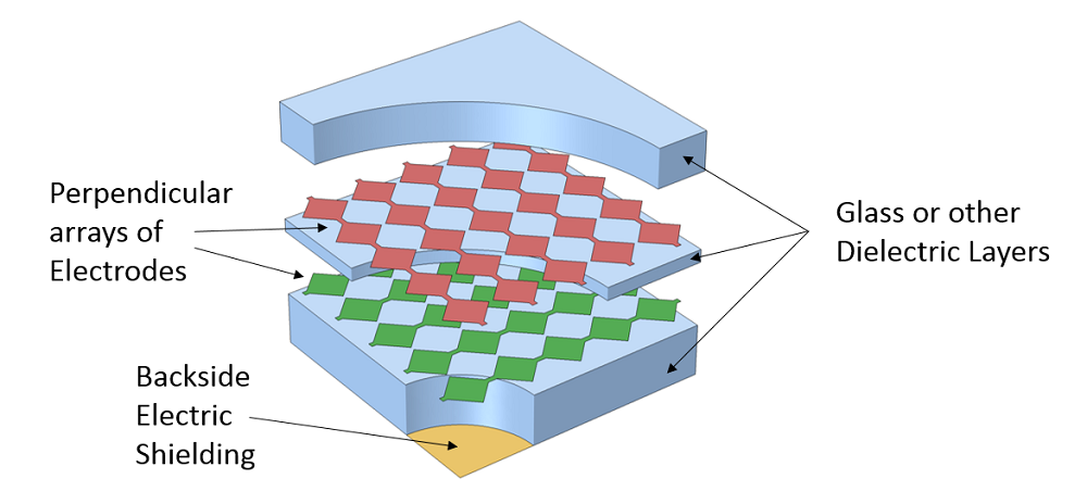
Let’s begin by considering a very elementary configuration that consists of two arrays of electrodes positioned at 90° to each other, as shown in the figure below.
Note that actual touchscreens are much more complex than what we will show here, but the modeling techniques will essentially be the same.

Simplified schematic of the key parts of a capacitive touchscreen sensor (not to scale).
An electrostatic field results whenever a voltage differential is applied between any two or more electrodes. Although the field is highest in the region between and around the electrodes, it does extend some distance away. When a conductive object (such as a finger) comes close to this region, the fields are altered and it becomes possible to sense the resultant capacitance change between the two active electrodes. It is this difference in capacitance that can be used to sense the position of a finger touching the screen.
While a subset of the electrodes has a potential difference applied, the other electrodes will either each be individually electrically isolated or they will all be electrically joined together — but still electrically isolated. Thus, they will be at a constant but unknown potential.
Correctly modeling these electrodes, as well as the surrounding metallic housings and other dielectric objects, is key to computing the capacitance changes. Let’s take a look at how to do this using the capabilities of the AC/DC Module.
Model of a Capacitive Sensor on a Wristwatch
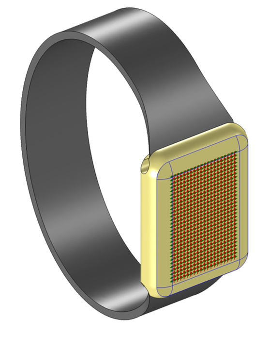
For this relatively small device, we can reasonably model the entire structure; the sensor is only 20 x 30 millimeters in size and the spacing between the electrodes is 1 millimeter. For larger touchscreens, it would be more reasonable to consider just a small subsection of the entire screen.

A capacitive sensor is embedded within the glass watch face (clear). The wrist band and watch case are only for visualization purposes.
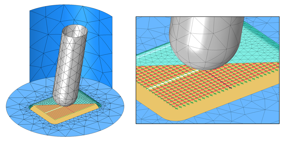
As shown in the following figures, the modeling domain is a cylindrical region. This region encompasses the glass screen, the finger, and an air volume around the watch. It’s reasonable to argue that the effect of the size of the surrounding air volume rapidly drops off as the size increases.
Boundary Conditions Used
Here, the boundaries of the air volume are set to a zero charge condition, mimicking a boundary to free space. Moreover, one of the bottom electrodes is set to the Ground boundary condition, fixing the voltage to zero. The Terminal boundary condition is applied to one of the electrodes on the top layer, which fixes it to a constant voltage. The Terminal boundary condition will also automatically compute the capacitance of this electrode. All of the other electrode boundaries are modeled via the Floating Potential boundary condition.

Visualization of the finite element model. The finger (gray), electric shielding (orange), and all unexcited electrodes (red and green) are modeled with floating potential boundary conditions. Two electrodes (white and black) have a potential difference applied. The watch face (cyan) is partially hidden. Electric insulation boundary conditions (blue) are used on all other faces. The air and the watch face are volume meshed. For clarity, the mesh is only shown on some surfaces.
The Floating Potential boundary condition is used to represent a set of surfaces over which a charge can freely redistribute itself. The condition is meant to simulate the boundaries of an object that will be at a constant but unknown electric potential. This is a consequence of an externally applied electrostatic field.
Several groups of faces use this Floating Potential boundary condition such as the bottom face of the watch, which represents the electric shielding underneath the glass cover. The electrodes that are not currently being excited are part of a single Floating Potential boundary condition (under the assumption that they are all electrically connected). Note that it’s possible to use the Floating Potential Group option to allow each physically separate boundary to float to a different constant voltage. It is also possible to electrically connect any set of electrodes simply by making them part of the same Group.
The boundaries of the finger (when it’s included in the model) also have the Floating Potential boundary condition. This is under the assumption that the human body is a relatively good conductor in comparison to the air and dielectric layers.
Materials Used
There are just two different materials being used here. The built-in Air material is applied to most domains and sets the permittivity to unity. The built-in Quartz Glass material is used to assign a higher permittivity to the screen.
Although the screen itself is a sandwich of different materials, we can assume that all layers have the same material properties. Hence, we do not need to explicitly model the boundaries between them; all the different layers are treated as a single domain.

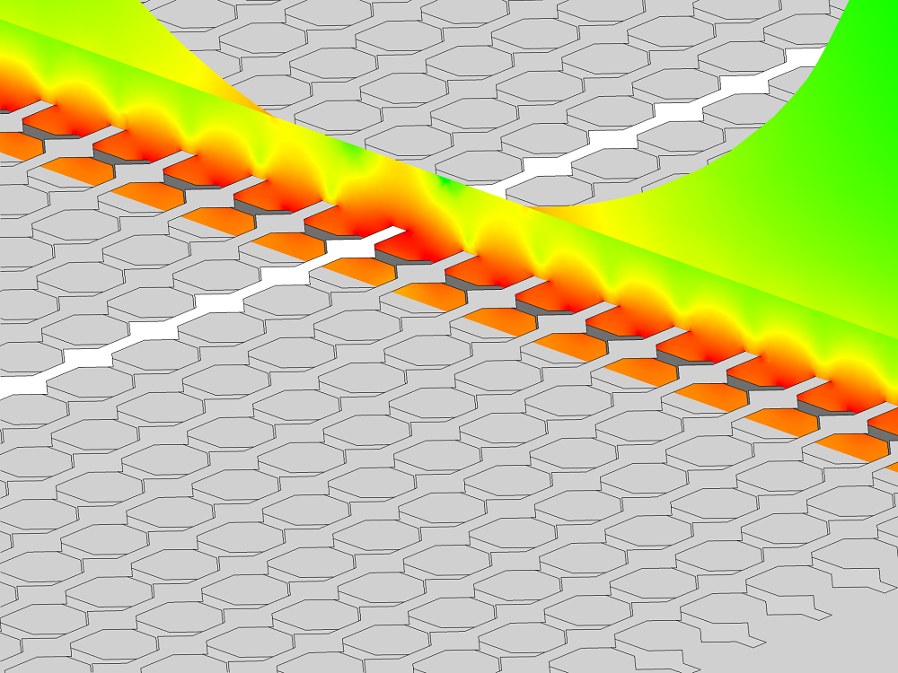
Color visualization of the log of the magnitude of the electric field. Since the finger is treated as a floating potential, the field inside is omitted.
Accurate Solutions Using Adaptive Mesh Refinement
Accurate results depend on having a finite element mesh that’s fine enough to resolve the spatial variations in the voltage field. Although we do not know ahead of time where the strong variations in the field will be, we can use adaptive mesh refinement to let the software determine where the smaller elements are needed.
Several levels of adaptive mesh refinement are used, and the results are presented in the table below. They were generated on an eight-core Intel® Xeon® processor running at 3.7 GHz, with 64 GB of RAM:
| Degrees of Freedom (millions) | Memory Used (GB) | Solution Time, Excluding Remeshing (seconds) | Percentage Difference in Measured Capacitance |
|---|---|---|---|
| 0.125 (Default “Normal” mesh setting) | 1.7 | 10 | 28% |
| 0.6 (After 1st adaptive mesh refinement) | 2.2 | 20 | 6% |
| 2.3 (2nd refinement) | 4.8 | 84 | 2% |
| 7.7 (3rd refinement) | 14 | 711 | 0.6% |
| 24.4 (4th refinement) | 47 | 2960 | N/A |
From the table above, we can deduce that we can start with a very coarse mesh and use adaptive mesh refinement to get a more accurate value of capacitance. This can be done at the cost of increased memory usage and solution time. The percentage difference in capacitances is compared to the most refined case.
Computing the Capacitance Matrix
So far, we have just looked at computing the capacitance between two of the electrodes in the array. In practice, we want to compute the capacitance between all of the electrodes: the Capacitance Matrix. This square symmetric matrix defines the relationship between applied voltage and charge on the electrodes in the system. For a system composed of n electrodes and one ground, the matrix is:
The diagonal components of this matrix are computed by taking the integral of the electric energy density over all domains:
where
The off-diagonal terms are given by:
where
These diagonal and off-diagonal terms are computed automatically by the software — but more on that in a later blog post.
Summary
We’ve looked at an example of a capacitive touchscreen device that was solved using the electrostatic modeling capabilities of the AC/DC Module. Although the geometry had been simplified for presentation purposes, the techniques outlined here can be used for more complex structures.
Whenever solving such finite element models, it will always be important to study the convergence of the desired quantities (in this case, usually the capacitance with respect to mesh refinement). The adaptive mesh refinement functionality greatly automates this model validation step.
When solving such large models, you can also benefit from using a distributed memory parallel solver for faster solution times. There is, of course, much more that you can do with COMSOL Multiphysics and the AC/DC Module than what is covered here.


Comments (7)
Oscar Diaz
October 12, 2015Dear Walter,
I’m working in an 3D electrostatic model with several electrodes (surfaces) at different potentials. I usually estimate each capacitance by evaluating the electric energy density integral obtained while having only one electrode with a potential U=1V and the rest at U=0V (GND). It looks like that when I use the BD condition terminal and run Results/Derived values/Global evaluation, I can also determine directly the capacitance value of one electrode at the time and also the equivalent electric charge (which should follow Q=CU). My questions are:
– is this global evaluation actually doing the electric energy density integral (couldn’t found a reference about it in the forums/blog/support neither in the comsol documentation)
– how can I obtain the capacitance matrix for the whole electrode arrangement I have?
Thanks.
Walter Frei
October 14, 2015 COMSOL EmployeeDear Oscar,
Yes, this global evaluation does actually integrate the electric energy density over all domains, as shown in the equations in this blog.
With regards to computing the entire capacitance matrix, please look into the “Terminal Sweep” functionality, it does what you are asking about.
Siddharth Krishnamoorthy
March 31, 2016Dear Walter,
Are there any tutorials that you might have or can point me to for finding the capacitance matrix in a multiple conductor system using the terminal sweep feature? I’m able to run the feature but I suspect I’m not seeing the right answer and I have no clue why without having some reference to look at.
Thank you very much,
Siddharth
yp zhao
April 21, 2017The off-diagonal terms, for the formula to compute Cij, for the coefficient 2/ViVj*W, I think it should be 1/ViVj*W, would you please double-check and confirm this?
Walter Frei
April 21, 2017 COMSOL EmployeeDear YP,
Thank you for that comment, the blog has been corrected. The product documentation and the formulae used within the software did always use the correct expression.
Best Regards,
Toyab Rahman
May 9, 2017Dear Walter,
Thanks for your wonderful post. I’m a fan of COMSOL Multiphysics. Actually, I’m working on energy harvesting mechanism where Triboelectric nanogenerator (TENG) is a popular trend on energy harvester field. There are several scientific renowned journals where they used COMSOL Multiphysics for simulating triboelectric properties. However, I haven’t found any post or application or any topic related to triboelectric nanogenerator or even triboelectric properties. I’m just wondering why there is no post or topic from COMSOL Inc.!
Caty Fairclough
May 9, 2017Dear Toyab,
Thank you for your comments.
We always welcome suggestions for new blog topics and have added your request to our list. It is good to hear that several researchers have already published work in this area using COMSOL, of course! If you’d like to share those references, I’m sure our team will find them useful.