- Bridging the Terahertz Gap
- Modeling the Lithium-Ion Battery
- Protection contre la Corrosion
- Modélisation des batteries
- Modélisation et Simulation dans le développement des piles à combustible
- Modélisation thermique des petits satellites
- Analyse électro-vibroacoustique d'un transducteur à armature équilibrée
Simulating Ideal and Experimental Impedance Response of Interdigitated Printed Circuit Boards
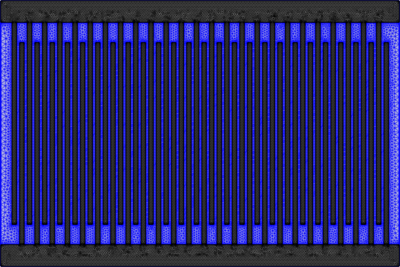
Large-scale manufacturing of electronic components require efficient forms of quality testing to ensure bulk fabrication and processing is performed to standard. With numerical simulations, the ideal behavior of such components may be evaluated to better know what to expect. Interdigitated printed circuit boards (PCBs) were simulated to assess ideal impedance responses under varying temperature and relative humidity conditions. The experimental samples compared have copper printed leads on FR4 boards with variation in the application of solder mask, while simulations assumed perfect geometries. The two variations are referred to as coated and uncoated boards. Coated boards have solder mask of roughly the same thickness on the entirety of the PCB, while uncoated boards exhibited multiple regions of varied solder mask thickness in repeating cycles throughout the circuits. This may be due to an error during a negative masking procedure for removing solder mask over the copper combs only. Electrical behavior is derived by utilizing the two-port admittance response gathered after applying two voltage terminals in the Electric Circuits (ec) physics module then converting to impedance. Simulations using copper leads on bare FR4 using the Built-in Material Library are first done due to the exact formulation of the solder mask being unknown. Solder mask properties are then derived by applying a coating of Blank Material over the interdigitated combs and FR4 and setting new material parameters to match that of the experimental results of the coated boards at ambient environmental conditions. To simulate those conditions, Heat and Moisture Multiphysics is performed by utilizing the Heat Transfer in Moist Air (ht) and Moisture Transport in Air (mt) physics modules. A spherical infinite element domain is introduced, where Built-in Material properties for Air is applied to a solid sphere surrounding the PCB. Once ambient properties are normalized for, simulations are performed at varying conditions and compared with experimental impedance responses. The same can then be done for the uncoated boards of greater complexity due to the variations in solder mask thickness. During experiments, topographical characterization using a Keyence 3D Surface Profiler microscope revealed that the solder mask on the held significant levels of porosity, a feature that is further adjusted for in the heat and moisture setups. It is expected for simulations to vary with experimental results due to discrepancies in apparent interdigitated comb heights, large peaks or pores of solder mask, and variation in solder mask application throughout the circuits. The accuracy of final uncoated board simulations with experimental results will boast the usefulness of these methods in making determinations for potential products. With simulations like these, the need for large quantities of demo batches can be reduced significantly.


